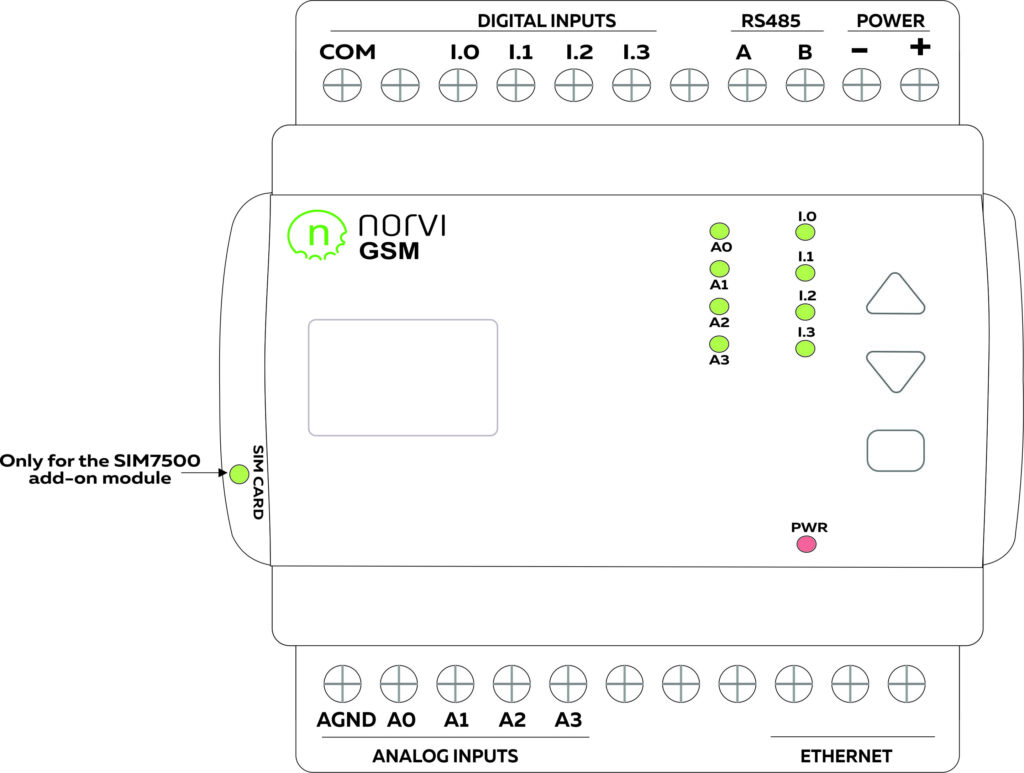
Product Features #

- ESP32-WROOM32 Module
- LTE Connection
- Built-in 0.96 OLED Display
- microSD Card Support
- DS3231 RTC with Battery Backup
- Ethernet via W5500
- Built-in Button on the front panel
- Digital Inputs
- Analog Inputs
- DIN-Rail mount
Cellular Communication LTE1
- Module – QUECTEL EC25
- Brand Name – QUECTEL
- FCC ID 2AQ9M-SIM7500
- TAC – 86675804
Cellular Communication LTE2
- Module – SIM7500
- Brand Name – SIMCom
- FCC ID 2AQ9M-SIM7500
- TAC – 86147503
Expansions Supported
- Analog Input
- Digital Input
Main #
| Range of Product | NORVI GSM |
| Product type | Programmable Controller |
| Certifications | EN 61131-2:2007 EN 61010-1:2010+A1:2019 EN IEC 61010-2-201:2018 2014/30/EU- Electromagnetic Compatibility (EMC) Annex III, Part B, Module C |
| Rated supply voltage | 24V DC |
| Communication | WiFI / Bluetooth LTE / EDGE – Quectel EC25 LTE2 / EDGE – SIMCOM SIM7500 RS 485 |
| Inputs and Outputs | 4 x Digital Inputs 4 x Analog Inputs with 0-10V |
| Displays and Visual Indicators | 0.96 OLED Display and Indicators |
Complementary #
| Product Unified Code | NORVI GSM-AE08-V-L |
| Product Part Numbers | NORVI GSM-AE08-V-L |
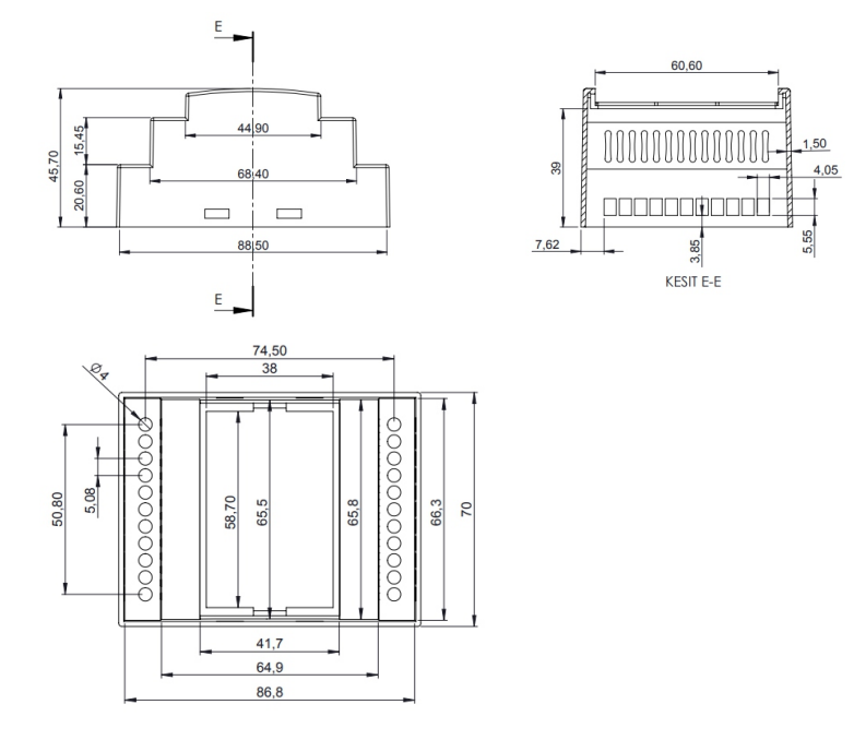
Mechanical Properties #
| Enclosure | NORVI 204 |
| Mounting / Installation Method | DIN RAIL / MOUNTING TABS |
| Terminal Type | SCREW TERMINAL |
| Terminal Arrangement | Top and Bottom |
| Length | 90.50 mm |
| Height | 56.60 mm |
| Width | 60.60 mm |
Environment #
| IP degree of protection | IP20 |
| Operating altitude | 0 – 2000 meters |
| Operating Temperature | – –10 … +85° C (14…185 °F) |
| Storage altitude | 0 – 3000 meters |
| Shock resistance | 15 gn for 11ms |
| Resistance to electrostatic discharge | 4kV on contact 8kV on air |
| Resistance to electromagnetic fields | 10 V/m (80 MHz …… 1GHz) 3 V/m (1.4 MHz …… 2 GHz) 1 V/m (2 MHz …… 3 GHz) |
Electrical Characteristics #
Grid Powered Devices #
| Rated Supply Voltage (V) | 24V DC |
| Current Consumption (mA) | 400mA |
| Recommended Power Source | 1A, 24V DC |
Processing #
| SOC / MCU | ESP32-WROOM32 |
| Flash Memory | 4MB |
| ROM | 448 KB |
| SRAM | 520 KB |
| PSRAM | NOT AVAILABLE |
Indicator Layout #
Peripherals #
microSD Card support #
| Card Type | microSD |
| Interface | SPI |
| SD CARD CS | GPIO15 |
| MISO | GPIO19 |
| MOSI | GPIO23 |
| SCLK | GPIO18 |
| SD Detect | NOT CONNECTED |
Internal RTC #
| RTC Chip | DS3231 |
| Backup Battery Type | CR2032 |
| Interface | I2C |
| I2C Address | 0x68 |
| SCL Pin | GPIO17 |
| SDA Pin | GPIO16 |
Built-in Buttons #
| Button 1 Pin | GPIO36 Analog Input Level 1 |
| Button 2 Pin | GPIO36 Analog Input Level 2 |
| Button 3 Pin | GPIO36 Analog Input Level 3 |
OLED Display #
| Display Driver | SSD1306 |
| Display Size | 0.96 inch |
| SCL Pin | GPIO17 |
| SDA Pin | GPIO16 |
| RESET Pin | NOT CONNECTED |
INPUTS and OUTPUTS #
Digital Inputs #
| Number of Digital Inputs | 5 |
| Digital Input Polarity | Sink and Source |
| Digital Input Maximum Voltage | 32V DC |
| Digital Input Minimum Voltage | 18V DC |
| Maximum Switching Frequency | 1 kHZ |
| Terminal Arrangement | Digital Input 1 – GPIO34 Digital Input 2 – GPIO35 Digital Input 3 – GPIO14 Digital Input 4 – GPIO13 Digital Input 5 – GPIO4 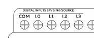 |
Analog Inputs #
| Number of Analog Inputs | 4 |
| Analog Input Measurement Range | 0-10V |
| Analog to Digital Converter (ADC) | ADS1115 |
| Analog to Digital Converter (ADC) Communication | I2C |
| Analog to Digital Converter (ADC) Address | 0x48 |
| Terminal Arrangement | A0 : Analog Input 0 – ADS1115 – 0x48 – AIN0 A1 : Analog Input 1 – ADS1115 – 0x48 – AIN1 A2 : Analog Input 2 – ADS1115 – 0x48 – AIN2 A3 : Analog Input 3 – ADS1115 – 0x48 – AIN3 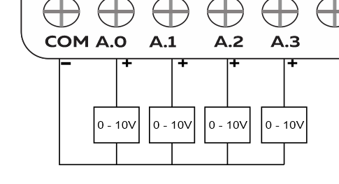 |
Communication Channels #
RS-485 Communication #
| Communication Mode | HALF-DUPLEX |
| Transceiver | MAX485 |
| Unit Load | 1/4 |
| Flow Control / Direction Control Pin | GPIO22 |
| TX Pin | GPIO26 |
| RX Pin | GPIO25 |
| Terminal Arrangement | 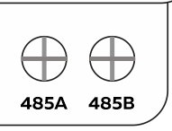 |
Ethernet SPI – W5500 #
| Transceiver | W5500 |
| Speed | 10BaseT/100BaseTX |
| Supports Auto Negotiation | Yes |
| TX/RX Buffer Size | Internal 32 Kbytes Memory |
| Supported Hardwired TCP/IP Protocols | TCP, UDP, ICMP, IPv4, ARP, IGMP, PPPoE |
| Number of Simultaneous independent sockets | 8 |
| SCSn | GPIO5 |
| MISO | GPIO19 |
| MOSI | GPIO23 |
| SCLK | GPIO18 |
| RSTn | GPIO22 |
| INTn | GPIO2 |
LTE Communication #
| Model of GSM Modem | QUECTEL EC25-E |
| FCC ID | XMR202008EC25AFXD |
| TAC | 86675804 |
| RXD | GPIO33 |
| TXD | GPIO32 |
| RESET | GPIO21 |
| Model of GSM Modem | SIM7500 |
| FCC ID | 2AQ9M-SIM7500 |
| TAC | 86147503 |
| RXD | GPIO33 |
| TXD | GPIO32 |
| RESET | GPIO21 |
GPIO Map #
| GPIO | Description | Usage |
| 0 | outputs PWM signal at boot | NRST |
| 1 | debug output at boot | TX0 |
| 2 | connected to on-board LED | INTn |
| 3 | HIGH at boot | RX0 |
| 4 | input only | Digital Input 5 |
| 5 | outputs PWM signal at boot | SCSN |
| 6 | connected to the integrated SPI flash | |
| 7 | connected to the integrated SPI flash | |
| 8 | connected to the integrated SPI flash | |
| 9 | connected to the integrated SPI flash | |
| 10 | connected to the integrated SPI flash | |
| 11 | connected to the integrated SPI flash | |
| 12 | boot fail if pulled high | |
| 13 | input only | Digital Input 4 |
| 14 | input onlyt | Digital Input 3 |
| 15 | outputs PWM signal at boot | SD CARD CS |
| 16 | SDA | |
| 17 | SCL | |
| 18 | SCLK | |
| 19 | MISO | |
| 20 | ||
| 21 | GSM RESET | |
| 22 | RS485-Flow Control | |
| 23 | MOSI | |
| 24 | ||
| 25 | RS485-RX | |
| 26 | RS485-TX | |
| 27 | ||
| 28 | ||
| 29 | ||
| 30 | ||
| 31 | ||
| 32 | GSM TX | |
| 33 | GSM RX | |
| 34 | input only | Digital Input 1 |
| 35 | input only | Digital Input 2 |
| 36 | Buttons | |
| 37 | ||
| 38 | ||
| 39 |
Expansion Port #
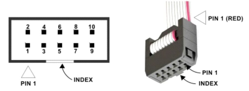
| PIN | ESP32 Connection |
| 1 | NOT CONNECTED |
| 2 | NOT CONNECTED |
| 3 | 5V |
| 4 | NOT CONNECTED |
| 5 | BOOT GPIO0 |
| 6 | NOT CONNECTED |
| 7 | 3.3V |
| 8 | SCL2 GPIO17 |
| 9 | GND |
| 10 | SDA2 GPIO16 |


